
RFID System Simulation
Info
We will describe how to simulate the wireless communication chain of a phase-shift keyed (PSK) modulated radio freqeuncy identification (RFID) system in Matlab. We endeavour to provide the mathematical equations and corresponding Matlab code to model the transmitter, wireless channel, analog front-end, and a digital baseband receiver of a RFID system.
Repository
The repository consists of the following:
- Matlab Codes for simulation of RFID system
The project structure is as follows:
RFID-System-Simulation
├── PSKSim.m           # main file consisting of all simulation parameters
├── constellation.m    # defines the PSK constelation map and bit encoding
├── channel.m          # computes antenna channel model
├── ADPLL_degree.m     # implements phase-locked loop
└── Subaxis            # helper module for plotting
    ├── parseArgs.m    # helper function for parsing varargin
    └── subaxis.m      # create axes in tiled positions
The following tools will be used to execute the simulation:
- Matlab R2015a
All equations, models, and algorithms in this repository were derived, verified, and written in Matlab manually without using any off-the-shelf black-box libraries.
Model
Any questions through email on the simulation is much welcomed.
The main file in this simulation model is named PSKSim.m. To begin, simply run this main file with the preset default simulation parameters. It will plot various graphs visualizing the entire signal transmission from the transmitter to the symbol decision stage.
The default simulation parameters should succesfully detect the start/end of the data packet, equalize the signal, and yield zero decoding bit error. The following will be printed in the Matlab command window,
Error check
Num of symb err: 0
signifying succesful completion of simulation.
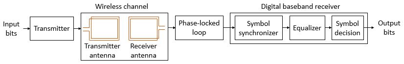
The wireless communication chain that is simulated in this project includes:
- transmitter
- wireless channel and antenna model
- phase-locked loop
- digital baseband receiver consisting of (i) symbol synchronizer, (ii) equalizer, and (iii) symbol decision, blocks.
Transmitter
The transmitter simulates M-ary PSK signal at carrier frequency fc and at data rate of fc/4. The constellation.m file defines the PSK constellation map on the complex plane and symbol bit encoding. Differential encoding is used to counter cycle slips.
The transmitter generates signal of the form:
- initial silence period (unmodulated sinusoidal signal)
- preamble or header (signifying the start of data packet)
-
Ndifferentially encoded PSK symbols (payload data) - end of packet symbol sequence (signifying end of data packet)
- final silence period (unmodulated sinusoidal signal)
NRZ (non-return to zero) pulse shaping is used at the transmitter.
Default simulation parameters for the transmitter are:
N = 800;                       % Number of symbols transmitted
M = 16;                        % M-ary PSK order
fc = 13.56e6;                  % Carrier frequency, units: Hz
dataRate = fc/4;               % Symbol rate or Baud rate
nSampSim = 32;                 % Number of samples per symbol for simulating transmitter and channel
nSamp = 2;                     % Number of samples per symbol for simulating receiver
TsSim = 1/(nSampSim*dataRate); % Sample time for simulating transmitter and channel
Ts = 1/(nSamp*dataRate);       % Sample time for simulating receiver
Note that the simulation involves multirate sampling. The transmitter and wireless channel are simulated at 16x faster at TsSim compared to the digital baseband receiver which is simulated at Ts.
Wireless Channel & Antenna Model
Wireless channel consists of trasmitter antenna, wireless transmission medium of air, and receiver antenna. The transmitter and receiver antenna circuit is modelled as series and parallel RLC circuit, respectively. Refer to Karris1 chapter 2, for detailed derivation of each individual circuit transfer function and antenna quality factor $Q$.
For all practical purposes, given that the separation between the transmitter and receiver is normally less than 10cm in an RFID application, we can model the wireless channel as mutually coupled pair of transmitter and receiver antenna coils. This leads to an equivalent circuit where the inductors are coupled via mutual inductance $M=k\sqrt{L_t\times L_r}$. Here, $k$ is the coefficient of coupling and provides a measure of the proximity of the primary and secondary coils, with values typically between 0.03 and 0.3. The value of $k$ is exactly unity only when the two coils are coalesced into a single coil.
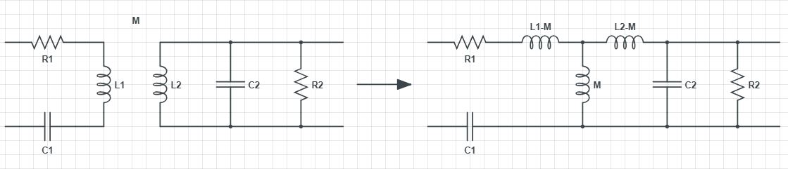
The overall Laplace $s$ domain bandpass transfer function of combined resonantor channel is given as
\[\begin{align} \frac{C_1MR_2s^2}{\left[ \begin{array}{c} R_2 + L_2s - C_1M^2s^3 + C_1L_1L_2s^3 + C_1L_1R_2s^2 + C_1L_2R_1s^2 + C_2L_2R_2s^2 + \\ C_1R_1R_2s - C_1C_2M^2R_2s^4 + C_1C_2L_1L_2R_2s^4 + C_1C_2L_2R_1R_2s^3 \end{array} \right]} \end{align}\]Symbolic derivation of the transfer function of resonator channel is shown on lines 7 - 20 in channel.m file. Mutual inductance, flux linkage, and equivalent circuit equations are further elaborated by Karris1 in chapter 8.
The analog bandpass channel transfer function is then mapped to digital lowpass equivalent. There are two methods to achieve this.
Method 1, follows the procedures described by Jeruchim2, page 143. Poles located on the negative-frequency half of $s$-plane are discarded and poles located on the positive-frequency half $s$-plane is shifted to the zero axis by substituting $s \rightarrow s+jw$. The transfer function is then discretized from $s$ domain to discrete $z$ domain.
Method 2, follows the procedures described by Farhang3, page 50. First, discretize the Laplace domain transfer function to obtain discretized transfer function. Then, substitute $z^x \rightarrow z^x\exp\left(j2\pi f_cT_sx\right)$ in the z-domain transfer function of the passband channel. Here, $f_c$ is the carrier frequency to donwconvert and $T_s$ is the sampling time. Example of Matlab implementation is given on page 364 of the book by line $c=c.^\star\exp(-j2\pi[0:length(c)-1]’\times T_{s}f_{c})$ where $c$ is the channel, $T_s$ is the sample time, and $f_c$ is the carrier frequency.
Both methods are implemented in channel.m file and visualized in the following figure.
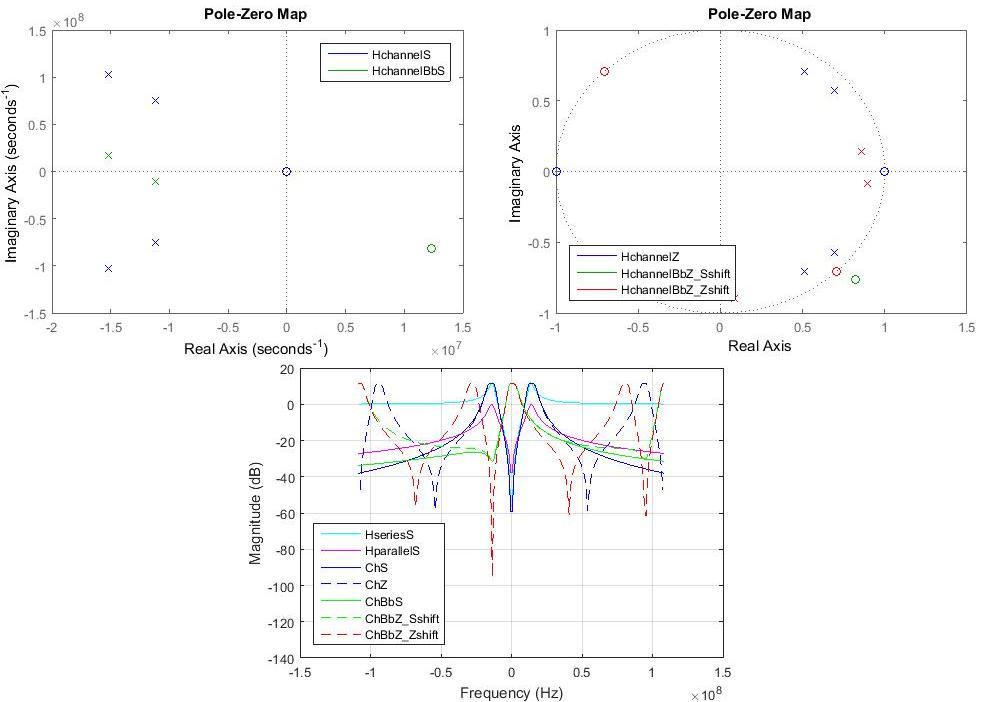
Frequency response of method 1 and method 2 around the zero frequency region (i.e., region of interest) is similar and matches that of Laplace $s$ domain equivalent lowpass transfer function.
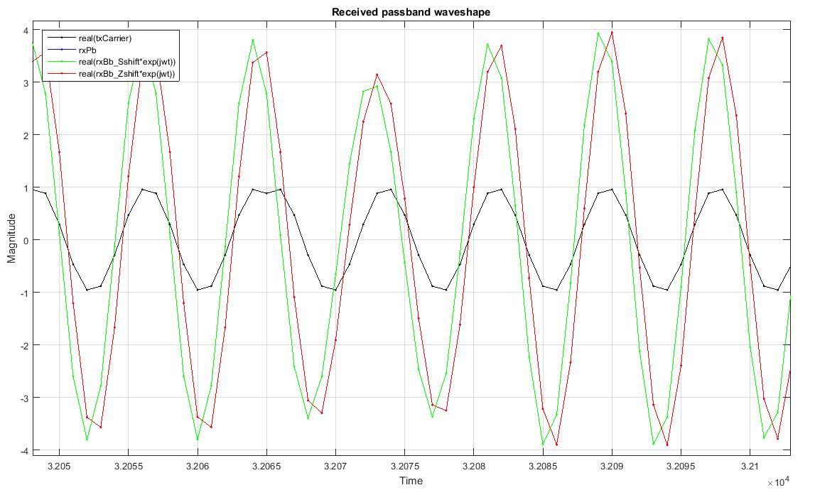
The received modulated passband waveshape at the receiver after propagating through the transmitter and wireless channel is depicted below.
Default simulation parameters for the wireless channel and antenna model are:
k = 0.3;         % 0<=k<=1; k is usually between 0.03 and 0.3
Qr = 4;          % Quality factor of transmitter antenna
Qc = 3;          % Quality factor of receiver antenna
fresr = 13.56e6; % Resonance frequency of transmitter circuit
fresc = 14e6;    % Resonance frequency of receiver circuit
Phase-Locked Loop (PLL)
Phase of the wireless-channel output is extracted using a PLL at the analog front-end of the receiver. The PLL simulation in ADPLL_degree.m file uses a second order digital PLL model consisting of a
- time-to-digital converter (TDC),
- loop filter (LF),
- digitally controlled oscillator (DCO), and
- frequency divider.
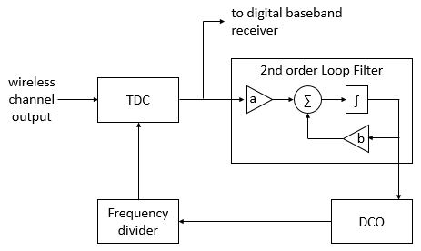
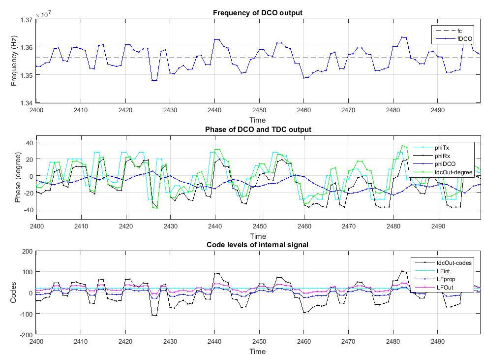
PLL attempts to synchronize the phase and frequency of its DCO with that of the input signal. In our simulation, the DCO operates at Ndiv times higher frequency than that of the incoming signal, hence a frequency divider is employed after the DCO. TDC compares the phase of the incoming signal with the phase of the frequency divider’s output. Once the DCO successfully tracks the incoming signal, the output of TDC matches the phase of information symbols transmitted. The extracted phase is then outputted to the digital baseband receiver block and also to the LF. LF low-pass filters the phase signal and produces an error signal to control the DCO. A second order LF is used, as both phase and frequency of DCO could be offset from that of the incoming signal.
Our PLL simulation model include quantization noise, saturation noise, and phase wrapping. Signal levels are quantized to the nearest integers (code levels) whereas large signals are clipped causing saturation noise.
Interested readers are referred to W. Tranter4 who provides excellent intuitive development of PLL models with accompanying MATLAB codes.
Default simulation parameters for the PLL are:
rpPLLdegree.Ndiv = 8;                    % frequency divider ratio in DCO
rpPLLdegree.Ktdc = (2^9 - 1)/180;        % map 180 degrees to 511 codes. Ktdc = 2.84
rpPLLdegree.Kdco = rpPLLdegree.Ndiv*3e3; % DCO gain, units: s^-1
rpPLLdegree.a = 1/4;                     % value of proportional constant in loop filter
rpPLLdegree.b = (1/2048)/Ts;             % value of integral coefficient in loop filter
rpPLLdegree.fDCOn0 = 108.0e6;            % initial n-multiple frequency of DCO; ideal value should be rpPLLdegree.Ndiv*fc;
rpPLLdegree.phiDCO0 = 14;                % initial phase of DCO in degrees within [-180,180)
rpPLLdegree.quantizationEn = 1;          % include quantization noise in PLL model
rpPLLdegree.saturationEn = 1;            % include saturation noise in PLL model
rpPLLdegree.phaseWrapEn = 1;             % include phase wrapping in PLL model
Digital Baseband Receiver
PLL output is fed into the digital baseband receiver. First, a symbol synchronizer, in the form of a pseudo matched filter, is employed to detect the start of the data packet. Once the packet is detected, the recieved signal is propagated through an equalizer followed by a symbol decision block. Decisions are made using minimum Euclidean distance metric.
The equalizer is set in a decision-feedback fractionally-spaced equalizer configuration, as fractionally-spaced equalization achieves optimum matched filtering and symbol time synchronisation. A fractionally spaced equalizer outputs a single decision for each symbol sampled at a rate higher than the symbol rate.
Affine projection algorithm is utilised as the optimizer to update the weight vectors. Affine projection, a data reusing algorithm, is chosen due to its favourable properties:
- It has a complexity and a speed of convergence in-between least-mean square(LMS) and recursive least squares(RLS) algorithm.
- It provides ability to control the adaptation-speed, -magnitude, and misadjustment of the coefficients.
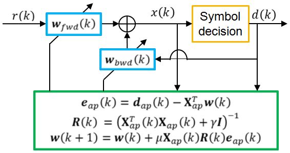
Refer to P.S.R. Diniz5, section 4.6 for detailed explanation of the affine projection algorithm, and table 4.5 for a summary of the algorithm steps.
The preamble of the data packet is used as training sequence by the equalizer. Once the payload data section is reached after the preamble, the symbol decisions made are outputted for the computation of bit error rate. Decoding by the digital baseband receiver is stopped when the end of packet symbol sequence is detected. Finally, the bit error rate is calculated and printed to screen by the simulation code.
Default simulation parameters for the digital baseband receiver model are:
kFwd_pos = 0:-1:-2;   % time index of received samples to be used as feed forward inputs in the equalizer
kBwd = 2;             % number of decision feedback inputs of the equalizer
mu = 0.25;            % convergence factor (step) (0 < mu < 1);
L = 2;                % data reuse factor (L=0 -> NLMS; L=1 -> BNLMS; ...)
gamma = 1;            % small positive constant to avoid singularity
bias = 0;             % default bias value of the equalizer
delay = 1;            % timesteps to be skipped between consecutive input data fed to the affine projection equalizer
fracEn = 1;           % enable fractionally spaced equalization
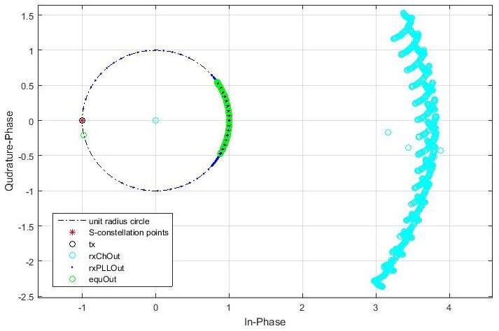
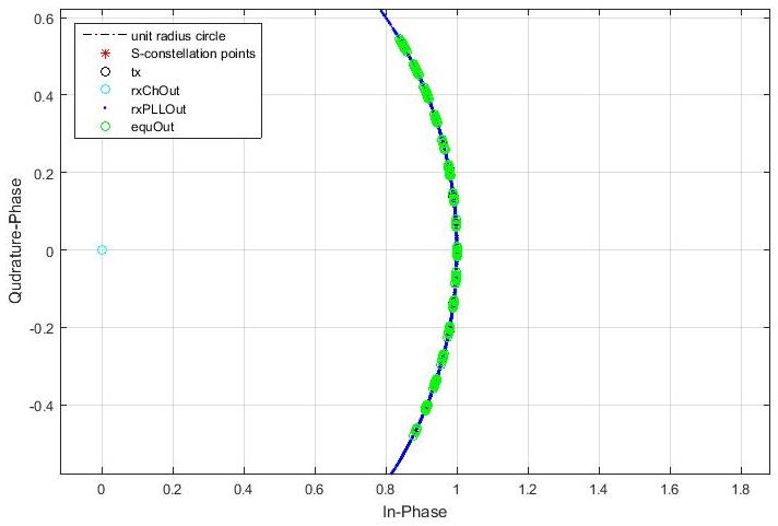
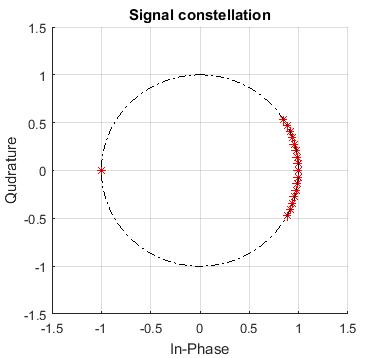
The figure above shows the information symbols plotted on the complex plane at various stages of transmission, beginning from the transmitter to the equalizer output. The signal points are heavily dispersed causing interysmbol interference (ISI) after propagation through the wireless channel. Then, PLL extracts the phase information of the symbols and outputs them on a unit-radius circle. The equalizer successfully clusters the symbol points into clearly separable groups of points, enabling the symbol decision block to easily decode the correct symbols using minimum Euclidean distance metric.
References
-
S.T. Karris, Circuit Analysis II with Matlab Applications, 2nd ed. Fremont California: Orchard Publications, 2003. ↩ ↩2
-
M.C. Jeruchim, P. Balaban, K.S. Shanmugam, Simulation of Communication Systems, 2nd ed. New York: Kluwer Academic Publishers, pp. 143, 2000. ↩
-
B. Farhang-Boroujeny, Signal Processing Techniques for Software Radios, 2nd ed. Lulu Publishing House, pp. 50, 2010. ↩
-
W. Tranter, R. Thamvichai, and Tamal Bose, Basic Simulation Models of Phase Tracking Devices Using MATLAB, Morgan & Claypool, 2010. ↩
-
P.S.R. Diniz, Adaptive Filtering - Algorithms and Practical Implementation, 4th ed. New York: Springer, pp. 162 - 168, 2013. ↩
Leave a comment